What Are Solar Panels Made Of? Complete Material Guide 2026
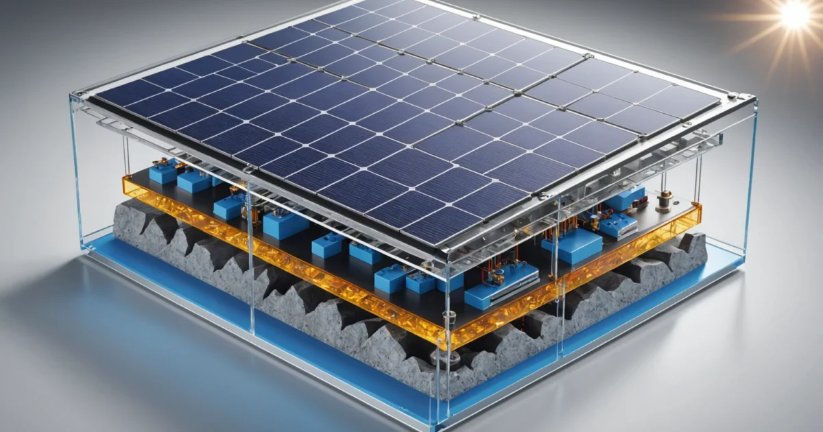
Solar panels are made out of several key materials including crystalline silicon as the primary semiconductor, tempered glass for protection, aluminum frames for structure, and various encapsulation materials like EVA (ethylene vinyl acetate). The core photovoltaic cells contain silicon wafers that are doped with phosphorus and boron to create electrical fields that convert sunlight into electricity.
Understanding these solar panel materials helps explain how photovoltaic systems work and their environmental impact. Most residential solar panels use monocrystalline or polycrystalline silicon cells, while commercial installations may feature thin-film technologies using cadmium telluride or copper indium gallium selenide.
Additionally, electrical components include silver and aluminum paste for contacts, copper ribbons for connections, and protective back sheets made from Tedlar or PET materials. These components work together to create durable systems with 25+ year lifespans while maintaining renewable energy efficiency.
TL;DR
- Silicon semiconductor cells (mono/polycrystalline) form the core photovoltaic material
- Protective layers include tempered glass, EVA encapsulant, and weather-resistant back sheets
- Structural components feature aluminum frames, silver/aluminum electrical contacts, and copper interconnects
- Alternative materials like cadmium telluride and CIGS are used in thin-film solar technologies
Core Solar Panel Materials: Silicon and Semiconductor Components
Crystalline silicon serves as the primary photovoltaic material in over 95% of solar panels worldwide. This semiconductor material converts sunlight into electricity through the photovoltaic effect, making it essential for renewable energy generation. Silicon’s abundance in Earth’s crust and proven performance make it the dominant choice for solar manufacturing.
Two main types of crystalline silicon dominate the market: monocrystalline and polycrystalline silicon. Monocrystalline panels feature uniform crystal structures that achieve higher efficiency rates of 20-22%, while polycrystalline variants offer cost-effective solutions with 15-17% efficiency. The manufacturing process determines these structural differences and performance characteristics.
Silicon Purification and Polysilicon Production
The silicon purification process begins with metallurgical-grade silicon extracted from quartz sand through high-temperature furnaces. Subsequently, manufacturers convert this raw silicon into polysilicon through chemical vapor deposition or the Siemens process. This purification achieves 99.9999% purity levels required for semiconductor applications.
Polysilicon production consumes significant energy but creates the foundation for all crystalline solar cells. Furthermore, this purified silicon undergoes crystal growth processes to form ingots, which are then sliced into thin wafers measuring 180-200 micrometers thick. These wafers become the base material for photovoltaic cell manufacturing.
Doping Agents: Creating Electrical Fields
Phosphorus and boron serve as essential doping agents that create the electrical fields necessary for photovoltaic operation. Phosphorus creates n-type silicon by adding extra electrons, while boron produces p-type silicon through electron deficiency. This doping process forms the p-n junction that generates electrical current when exposed to sunlight.
The doping concentration typically ranges from 1 part per million to 1 part per thousand, depending on the desired electrical properties. Additionally, manufacturers carefully control temperature and atmospheric conditions during the doping process to ensure uniform distribution throughout the silicon wafer. This precision directly impacts the solar cell’s efficiency and performance characteristics.
Doping Process Impact
Alternative Semiconductor Materials
Cadmium telluride (CdTe) represents the most commercially successful thin-film technology, accounting for approximately 5% of global solar panel production. CdTe panels offer lower manufacturing costs and better performance in high-temperature conditions compared to crystalline silicon. However, cadmium’s toxicity raises environmental concerns regarding disposal and recycling.
Copper indium gallium selenide (CIGS) provides another thin-film alternative with flexible application possibilities. CIGS technology achieves laboratory efficiencies exceeding 23% while maintaining good performance in low-light conditions. Nevertheless, the scarcity of indium and gallium creates supply chain challenges for large-scale production.
Amorphous silicon offers the lowest-cost semiconductor option for specific applications like calculators and small electronics. This non-crystalline form of silicon requires thinner layers but suffers from lower efficiency rates of 6-8%. Despite efficiency limitations, amorphous silicon performs well in diffuse light conditions and maintains stable output over time.
| Semiconductor Material | Efficiency Range | Key Advantages | Main Limitations |
|---|---|---|---|
| Monocrystalline Silicon | 20-22% | High efficiency, proven reliability | Higher manufacturing cost |
| Polycrystalline Silicon | 15-17% | Cost-effective, good performance | Lower efficiency than mono |
| Cadmium Telluride | 16-18% | Low cost, heat tolerance | Toxicity concerns |
| CIGS | 15-20% | Flexibility, low-light performance | Material scarcity |
| Amorphous Silicon | 6-8% | Lowest cost, diffuse light tolerance | Low efficiency |
Research continues into emerging semiconductor materials like perovskite and organic photovoltaics that could revolutionize solar technology. These next-generation materials promise higher efficiencies and lower costs, though stability and manufacturing scalability remain significant challenges. Current developments focus on tandem cell designs that combine multiple semiconductor layers for enhanced performance.
Protective Glass and Encapsulation Materials
Beyond semiconductor cells, solar panels require sophisticated protective materials that shield delicate components while maximizing light transmission. These encapsulation materials form critical barriers against moisture, temperature fluctuations, and mechanical stress. The protective layers determine panel longevity, with quality materials extending operational life beyond 25 years.
Tempered Glass Front Protection
Tempered glass serves as the primary protective barrier, typically measuring 3.2-4.0mm thick. This specialized glass undergoes thermal tempering processes that increase strength by 400-500% compared to standard glass. Manufacturers incorporate anti-reflective coatings that reduce surface reflection from 8% to less than 2%, significantly improving light transmission efficiency.
The glass composition includes low-iron content that minimizes light absorption in the blue spectrum. Furthermore, textured surfaces create microscopic patterns that scatter light, reducing glare while maintaining optical clarity. These anti-reflective properties directly impact energy output, with coated glass increasing panel efficiency by 2-3% compared to uncoated alternatives.
EVA Encapsulation Technology
Ethylene vinyl acetate (EVA) encapsulant protects solar cells through transparent polymer layers that bond during lamination. EVA demonstrates excellent optical properties with light transmission exceeding 95% across the solar spectrum. Additionally, this thermoplastic material provides cushioning that absorbs mechanical stress from thermal expansion and external impacts.
The encapsulation process involves heating EVA films to 150°C, creating cross-linked polymer networks that permanently seal cell assemblies. Quality EVA formulations include UV stabilizers and antioxidants that prevent degradation over decades of sun exposure. However, standard EVA can experience browning after 15-20 years, leading manufacturers to develop advanced formulations with improved UV resistance.
Alternative Encapsulant Materials
Thermoplastic polyurethane (TPU) offers superior flexibility and durability compared to traditional EVA encapsulants. TPU maintains optical clarity longer and resists yellowing under intense UV exposure. Consequently, premium solar panels increasingly utilize TPU for applications requiring enhanced longevity, particularly in harsh environmental conditions.
Polyvinyl butyral (PVB) provides another encapsulation alternative with excellent adhesion properties and moisture barrier performance. PVB demonstrates superior resistance to delamination, a common failure mode in solar panels exposed to humidity cycling. Nevertheless, higher material costs limit PVB adoption to specialized applications where maximum durability justifies the expense.
Back Sheet Protection Systems
Back sheet materials form the final protective barrier, shielding panels from moisture ingress and electrical hazards. Tedlar (polyvinylfluoride) represents the industry standard, offering exceptional chemical resistance and dielectric strength. Tedlar back sheets maintain integrity for 25+ years while providing electrical insulation exceeding 1000V.
Polyethylene terephthalate (PET) serves as a cost-effective alternative with good moisture barrier properties and UV stability. PET back sheets typically feature multi-layer constructions that combine different polymer films for optimized performance. Meanwhile, fluoropolymer back sheets deliver premium protection with superior chemical inertness and thermal stability, though at significantly higher costs.
Modern back sheet designs incorporate breathable membranes that allow trapped moisture to escape while preventing water ingress. These advanced materials balance protection with pressure equalization, reducing stress on laminated assemblies. Quality back sheets contribute significantly to panel dimensional stability and long-term reliability performance.
Material Recycling Considerations
Electrical Components and Metallization
Solar panels require sophisticated electrical systems to capture and transport the energy generated by photovoltaic cells. These electrical components transform light into usable electricity while ensuring efficient current collection and safe operation. Understanding these materials reveals how solar technology converts sunlight into power for homes and businesses.
Front-Side Contact Materials
Silver paste forms the primary material for front-side electrical contacts on solar cells. This conductive material creates the grid pattern visible on solar panel surfaces, collecting electrons generated by the photovoltaic effect. Silver demonstrates excellent electrical conductivity while maintaining stability under UV exposure and thermal cycling.
Screen-printing processes apply silver paste in precise patterns that maximize current collection while minimizing shading losses. The paste contains silver particles, glass frit, and organic binders that enable proper adhesion to silicon surfaces. During firing, temperatures reach 800°C, creating strong metallurgical bonds between silver and the semiconductor material.
Modern silver pastes incorporate advanced formulations that reduce material consumption while maintaining performance. Manufacturers continuously optimize particle size distribution and binder chemistry to achieve lower contact resistance. These improvements directly impact panel efficiency and manufacturing costs across the solar industry.
Back-Side Contact Systems
Aluminum paste serves dual functions on the back surface of solar cells, providing electrical contact and optical reflection. This material creates the back surface field that improves electron collection efficiency while reflecting unabsorbed light back through the silicon wafer. Aluminum’s lower cost compared to silver makes it ideal for full-area back contacts.
The aluminum metallization process involves screen-printing followed by high-temperature firing that creates aluminum-silicon alloy formation. This alloying process establishes excellent electrical contact while maintaining mechanical stability throughout the panel’s operational life. Additionally, aluminum’s reflective properties contribute to improved light trapping within the cell structure.
Some advanced cell designs incorporate silver-aluminum combinations for optimized back contact performance. These hybrid approaches balance conductivity requirements with cost considerations, particularly in high-efficiency cell architectures. The metallization quality directly affects power output and long-term reliability of solar panels.
Interconnection Materials
Copper ribbons connect individual solar cells within panels, forming series and parallel electrical pathways. These flat conductors typically measure 1.5-2.0mm in width with tinned surfaces that enable reliable soldering to cell contacts. Copper’s excellent conductivity and flexibility make it ideal for handling thermal expansion stresses.
Tabbing ribbons undergo careful design optimization to minimize electrical losses while maintaining mechanical durability. The ribbon thickness affects both conductivity and stress distribution across cell interconnections. Furthermore, proper ribbon routing prevents hot spots that could damage cells or reduce panel performance over time.
Bus ribbons provide higher current-carrying capacity for connecting cell strings to external terminals. These wider copper conductors feature enhanced cross-sectional areas that accommodate increased current flows. Quality interconnection materials contribute significantly to panel dimensional stability and electrical performance throughout the system’s lifespan.
Junction Box Components
Polycarbonate housing materials protect critical electrical connections within solar panel junction boxes. This thermoplastic polymer offers excellent impact resistance, UV stability, and flame retardant properties essential for outdoor applications. Polycarbonate maintains dimensional stability across wide temperature ranges while providing IP65 or higher ingress protection ratings.
Junction box designs incorporate multiple sealing systems that prevent moisture ingress and maintain electrical safety. The housing materials resist thermal cycling, UV degradation, and mechanical stress from cable connections. Additionally, polycarbonate’s electrical insulation properties ensure safe operation at system voltages up to 1500V DC.
Bypass diodes within junction boxes protect solar panels from reverse current flow and hot spot formation. These semiconductor devices typically use Schottky diode technology that provides low forward voltage drop and fast switching characteristics. Bypass diodes activate when individual cells become shaded or damaged, maintaining power output from unaffected portions of the panel.
Diode selection considers current rating, thermal management, and long-term reliability under outdoor conditions. Quality bypass diodes feature robust packaging that withstands temperature cycling and humidity exposure. These protective components prevent catastrophic failures that could damage entire solar installations, ensuring safe and reliable operation throughout the panel’s 25-year warranty period.
Structural Framework and Mounting Materials
The structural framework forms the backbone of every solar panel, providing mechanical support and environmental protection for delicate photovoltaic cells. Aluminum frames dominate modern solar panel construction due to their exceptional strength-to-weight ratio and natural corrosion resistance properties. These extruded aluminum profiles create rigid perimeter structures that protect glass surfaces while enabling secure mounting to rooftop or ground-based systems.
Aluminum’s inherent corrosion resistance stems from its ability to form a protective oxide layer when exposed to oxygen. This natural barrier prevents further oxidation and maintains structural integrity throughout decades of outdoor exposure. Furthermore, aluminum frames demonstrate excellent thermal expansion characteristics that accommodate temperature fluctuations without compromising panel alignment or seal integrity.
Anodized Aluminum Benefits
Anodized aluminum treatment enhances the natural corrosion resistance of standard aluminum frames through controlled electrochemical oxidation. This process creates a thicker, more durable oxide layer that provides superior weather protection compared to untreated aluminum surfaces. Anodized coatings resist salt spray, acid rain, and UV radiation while maintaining their protective properties for 25+ years.
The anodizing process also improves the aluminum’s aesthetic appearance and provides better paint adhesion for colored frame applications. Additionally, anodized surfaces demonstrate enhanced electrical insulation properties that prevent galvanic corrosion when aluminum frames contact dissimilar metals in mounting systems.
Stainless Steel Hardware Components
Stainless steel hardware provides the critical connection points between solar panels and their mounting structures. These components include bolts, nuts, washers, and specialized clamps that secure panels to rails or direct-mount systems. Grade 316 stainless steel represents the preferred material choice due to its exceptional corrosion resistance in marine and industrial environments.
Mounting hardware must withstand significant mechanical loads from wind uplift, snow accumulation, and thermal expansion cycles. Stainless steel’s high tensile strength and fatigue resistance ensure reliable connections throughout the system’s operational lifetime. Moreover, stainless steel components maintain their mechanical properties across extreme temperature ranges from -40°C to +85°C.
| Hardware Component | Material Grade | Primary Function |
|---|---|---|
| End clamps | 316 stainless steel | Secure panel edges to mounting rails |
| Mid clamps | 316 stainless steel | Connect adjacent panels together |
| Grounding lugs | 316 stainless steel | Provide electrical grounding path |
| Rail splices | 316 stainless steel | Join mounting rail sections |
Weatherproofing Sealants and Gaskets
Silicone-based sealants create weatherproof barriers between frame components and mounting hardware to prevent water infiltration. These elastomeric materials maintain flexibility across wide temperature ranges while providing excellent adhesion to aluminum, glass, and stainless steel surfaces. High-quality silicone sealants resist UV degradation, ozone exposure, and thermal cycling for decades of reliable performance.
Structural glazing silicones bond the glass surface directly to aluminum frames, creating continuous weatherproof seals around the panel perimeter. These sealants must meet stringent structural requirements while maintaining transparency and UV stability. Additionally, neutral-cure silicones prevent corrosion of metal components during the curing process.
EPDM rubber gaskets provide compression seals at frame joints and mounting interfaces where mechanical fasteners create potential leak paths. These synthetic rubber materials demonstrate exceptional weather resistance and maintain sealing pressure throughout thermal expansion cycles. EPDM gaskets also provide electrical isolation between dissimilar metals, preventing galvanic corrosion in mounting systems.
Quality weatherproofing materials ensure solar panels maintain their protective encapsulation throughout their 25-year warranty period. Proper sealing prevents moisture ingress that could cause delamination, corrosion, or electrical safety hazards. Therefore, manufacturers specify premium sealants and gaskets that exceed standard building material requirements for outdoor exposure.
Thin-Film Solar Panel Material Composition
Thin-film solar panels utilize different semiconductor materials compared to crystalline silicon panels, creating lightweight and flexible alternatives through advanced deposition techniques. These panels consist of extremely thin layers of photovoltaic materials applied to various substrate materials. Manufacturing processes deposit these semiconductor layers at thicknesses measuring only a few micrometers, significantly reducing material costs while maintaining energy conversion capabilities.
Cadmium Telluride (CdTe) Technology
Cadmium telluride represents the most commercially successful thin-film technology, accounting for approximately 5% of global solar panel production. CdTe panels utilize cadmium telluride as the primary absorber layer, deposited onto glass substrates through vapor transport deposition or close-space sublimation processes. These panels achieve conversion efficiencies between 16-22% while maintaining lower manufacturing costs than crystalline silicon alternatives.
The substrate materials for CdTe panels typically consist of soda-lime glass ranging from 3-4 millimeters in thickness. This glass provides structural support while allowing light transmission to reach the semiconductor layers. Additionally, manufacturers apply transparent conductive oxide coatings to the glass surface before depositing the cadmium telluride layer, creating the electrical contact necessary for current collection.
Copper Indium Gallium Selenide (CIGS) Composition
CIGS solar cells incorporate copper, indium, gallium, and selenium elements in precise stoichiometric ratios to form the light-absorbing layer. The composition typically follows the chemical formula Cu(In,Ga)Se₂, where gallium content determines the bandgap energy and affects the cell’s spectral response. Manufacturers control the gallium-to-indium ratio to optimize performance for specific applications, with higher gallium content increasing the open-circuit voltage.
CIGS deposition occurs through co-evaporation or sputtering processes onto flexible substrates such as polyimide films or stainless steel foils. These flexible substrates enable roll-to-roll manufacturing processes that reduce production costs. Furthermore, CIGS panels demonstrate excellent performance in low-light conditions and maintain efficiency across wide temperature ranges, making them suitable for diverse environmental conditions.
Amorphous Silicon Applications
Amorphous silicon (a-Si) thin-film panels utilize non-crystalline silicon deposited through plasma-enhanced chemical vapor deposition at temperatures below 300°C. This low-temperature process allows deposition onto various substrate materials including glass, plastic, and metal foils. Amorphous silicon absorbs light more efficiently than crystalline silicon due to its disordered atomic structure, requiring layer thicknesses of only 0.5-1.0 micrometers.
Glass substrates for amorphous silicon panels range from standard soda-lime glass to specialized low-iron glass that maximizes light transmission. Meanwhile, flexible substrate applications utilize polyethylene terephthalate (PET) or polyimide films that enable bendable solar panels for curved surfaces. These flexible panels find applications in building-integrated photovoltaics and portable electronic devices where conformability is essential.
Transparent Conductive Oxide Layers
Transparent conductive oxides (TCOs) serve as the front electrical contact in thin-film solar panels, collecting generated current while allowing light penetration to the absorber layer. Indium tin oxide (ITO) remains the most widely used TCO material due to its excellent electrical conductivity and optical transparency. ITO films typically achieve sheet resistances below 10 ohms per square while maintaining over 85% optical transmission in the visible spectrum.
Fluorine-doped tin oxide (FTO) provides a cost-effective alternative to ITO, particularly for large-area applications where indium scarcity affects material costs. FTO demonstrates superior thermal stability and chemical resistance compared to ITO, making it suitable for high-temperature processing steps. However, FTO exhibits slightly higher sheet resistance, requiring optimized layer thickness to balance conductivity and transparency requirements.
Both ITO and FTO layers undergo sputter deposition or chemical vapor deposition processes to achieve uniform thickness across large substrate areas. The deposition parameters control grain structure, carrier concentration, and mobility properties that determine the final electrical and optical performance. Moreover, these TCO materials must maintain stability under UV exposure and thermal cycling throughout the panel’s operational lifetime.
Understanding thin-film material compositions helps consumers evaluate different solar panel technologies based on efficiency, cost, and application requirements. For comprehensive information about renewable energy options and their environmental benefits, these material innovations continue advancing solar technology accessibility and performance across diverse markets.
Environmental Impact and Recycling of Solar Panel Materials
Solar panel materials create both environmental benefits and challenges throughout their lifecycle. While photovoltaic systems generate clean electricity for decades, their manufacturing processes and end-of-life disposal require careful environmental management. Understanding these impacts helps consumers make informed decisions about solar technology adoption.
Material Toxicity Concerns in Solar Manufacturing
Cadmium telluride thin-film panels contain toxic cadmium compounds that pose environmental risks during manufacturing and disposal. However, manufacturers implement strict containment protocols to prevent cadmium release during normal operations. Additionally, lead solder in older crystalline silicon panels creates disposal challenges, though newer panels increasingly use lead-free alternatives.
Heavy metals including silver, tin, and antimony appear in various panel components but remain safely encapsulated during normal use. Furthermore, silicon purification processes generate silicon tetrachloride waste that requires proper treatment to prevent environmental contamination. Nevertheless, modern manufacturing facilities implement closed-loop systems to minimize toxic waste generation.
Safety Note
Recyclability of Core Solar Panel Materials
Silicon wafers represent the most valuable recyclable component, containing over 95% pure silicon that can be reprocessed for new panels. Recycling facilities recover silicon through chemical etching processes that remove surface layers and dopants. Moreover, aluminum frames achieve nearly 100% recyclability through standard metal recycling processes.
Glass substrates comprise approximately 75% of panel weight and can be recycled into new glass products or construction materials. However, the laminated structure requires specialized separation techniques to remove polymer interlayers. Additionally, precious metals including silver and copper provide economic incentives for recycling due to their high material value.
| Material | Percentage by Weight | Recyclability |
|---|---|---|
| Glass | 75% | 95%+ |
| Aluminum | 10% | 100% |
| Silicon | 5% | 85% |
| Polymers | 7% | Limited |
| Metals | 3% | 90%+ |
End-of-Life Recovery Processes and Challenges
Thermal treatment represents the primary method for separating laminated panel components, using controlled heating to soften polymer layers. This process enables mechanical separation of glass, silicon, and metal components for individual recycling streams. However, thermal processing requires significant energy input and specialized equipment.
Chemical dissolution offers an alternative approach using solvents to break down polymer encapsulants without high-temperature treatment. This method preserves material quality but generates chemical waste requiring proper treatment. Furthermore, mechanical shredding provides a lower-cost option that produces mixed material streams suitable for construction applications.
Economic challenges limit widespread panel recycling due to relatively low material values compared to processing costs. Consequently, many end-of-life panels currently enter general waste streams rather than specialized recycling facilities. However, increasing panel volumes and regulatory requirements are driving investment in dedicated solar recycling infrastructure.
Sustainable Material Alternatives and Manufacturing Improvements
Perovskite solar cells utilize abundant materials including titanium dioxide and organic compounds, reducing dependence on rare elements. These emerging technologies demonstrate promising efficiency levels while using earth-abundant materials. Additionally, organic photovoltaics employ carbon-based materials that offer improved recyclability and reduced toxicity.
Lead-free solder alternatives including silver-copper alloys eliminate toxic lead from panel assembly processes. Meanwhile, manufacturers develop recyclable encapsulants using thermoplastic materials that simplify end-of-life separation. These innovations reduce environmental impact while maintaining panel performance and durability.
Manufacturing improvements focus on reducing energy consumption and waste generation throughout production processes. Closed-loop systems capture and reuse process chemicals, minimizing environmental discharge. For broader context on sustainable energy solutions, renewable energy technologies continue advancing environmental benefits across multiple sectors.
Solar panels offset their manufacturing environmental impact within 1-4 years of operation while generating clean electricity for 25+ years.
Research into bio-based materials explores using renewable feedstocks for panel components, potentially replacing petroleum-derived polymers with plant-based alternatives. These developments aim to create fully sustainable solar panels that minimize environmental impact from raw material extraction through end-of-life disposal.
Frequently Asked Questions
What are the raw materials in solar panels?
Solar panels contain several key raw materials including crystalline silicon as the primary semiconductor, tempered glass for protection, aluminum for frames, and EVA (ethylene vinyl acetate) for encapsulation. Additional materials include silver and aluminum paste for electrical contacts, copper ribbons for connections, and protective back sheets made from Tedlar or PET materials. The silicon wafers are doped with phosphorus and boron to create the electrical fields necessary for converting sunlight into electricity.
What is the lifespan of a solar panel?
Solar panels typically have a lifespan of 25-30 years or more. Most manufacturers provide warranties guaranteeing at least 80% of original power output after 25 years. The durable materials used in construction, including tempered glass, aluminum frames, and weather-resistant encapsulants, enable solar panels to withstand decades of outdoor exposure while maintaining renewable energy efficiency.
What happens after 25 years of solar panels?
After 25 years, solar panels typically still produce 80-85% of their original power output. They don’t suddenly stop working but gradually decline in efficiency. Many panels continue operating effectively for 30-40 years. At end-of-life, the materials can be recycled, with silicon, aluminum, glass, and copper being recoverable for new manufacturing processes.
Can solar panels be recycled?
Yes, solar panels can be recycled. The aluminum frames, tempered glass, and copper wiring are easily recyclable through standard processes. Silicon wafers can be reprocessed for new solar cells, and even the silver contacts can be recovered. Specialized recycling facilities can recover up to 95% of semiconductor materials and virtually all metal components, making solar panels environmentally sustainable at end-of-life.
Are solar panels harmful to the environment?
Solar panels have minimal environmental impact during operation and provide significant environmental benefits by generating clean, renewable energy. While manufacturing requires energy and some chemicals, the energy payback time is typically 1-4 years. Over their 25+ year lifespan, solar panels generate far more clean energy than was used in their production, resulting in a net positive environmental impact.
Are solar panels toxic to humans?
Standard crystalline silicon solar panels are not toxic to humans during normal use. The silicon, aluminum, glass, and other materials are safely encapsulated and pose no health risks. However, some thin-film technologies contain cadmium telluride, which requires proper handling during manufacturing and recycling. Residential and commercial installations using crystalline silicon panels present no toxicity concerns for occupants or installers.
What's the difference between monocrystalline and polycrystalline solar panels?
Monocrystalline panels feature uniform crystal structures that achieve higher efficiency rates of 20-22%, while polycrystalline panels offer cost-effective solutions with 15-17% efficiency. Monocrystalline panels are made from single silicon crystals, resulting in better performance and a distinctive black appearance. Polycrystalline panels use multiple silicon crystals, creating a blue-speckled appearance and lower manufacturing costs.
How are solar panels made step by step?
- Silicon purification: Raw silicon is purified to 99.9999% purity through chemical processes
- Crystal growth: Purified silicon is formed into ingots through controlled crystallization
- Wafer slicing: Ingots are sliced into thin wafers measuring 180-200 micrometers
- Doping process: Wafers are treated with phosphorus and boron to create electrical fields
- Cell assembly: Electrical contacts using silver and aluminum paste are applied
- Panel assembly: Cells are encapsulated in EVA, covered with tempered glass, and framed with aluminum
What are solar panels used for?
Solar panels are primarily used to convert sunlight into electricity for residential, commercial, and utility-scale applications. Common uses include powering homes and businesses, charging electric vehicles, providing electricity for remote locations, and feeding clean energy into the electrical grid. Solar panels enable energy independence while reducing reliance on fossil fuels and lowering electricity costs.
Why are people getting rid of their solar panels?
Most people don’t voluntarily remove functioning solar panels due to their long-term value. However, panels may be replaced during roof renovations, when upgrading to more efficient technology, or due to physical damage from severe weather. Some early adopters replace older, less efficient panels with newer technology to maximize energy production. End-of-life replacement typically occurs after 25-30 years of service.
What are thin-film solar panels made of?
Thin-film solar panels use alternative semiconductor materials including cadmium telluride (CdTe), copper indium gallium selenide (CIGS), and amorphous silicon. These materials are deposited in extremely thin layers on substrates like glass or flexible materials. CdTe represents the most commercially successful thin-film technology, while CIGS offers high efficiency potential for specialized applications.
How pure does silicon need to be for solar panels?
Silicon for solar panels requires 99.9999% purity (six nines purity) to function effectively as a semiconductor. This ultra-high purity is achieved through processes like the Siemens method or chemical vapor deposition. The purification removes impurities that would interfere with the photovoltaic effect, ensuring optimal electrical performance and efficiency in converting sunlight to electricity.
What is the environmental impact of solar panel materials?
The environmental impact of solar panel materials is overwhelmingly positive over their lifecycle. While manufacturing requires energy and some chemical processes, the materials enable decades of clean energy generation. Silicon is abundant and non-toxic, aluminum and glass are highly recyclable, and the overall carbon footprint is recovered within 1-4 years of operation. The 25+ year lifespan results in significant net environmental benefits compared to fossil fuel alternatives.
You May Also Like
Air-to-Air Heat Pumps (2026): Cost, Efficiency, Pros & Cons
Home Insulation Guide (2026): Types, R-Value, Cost & Savings

Best Portable Power Stations for Home Backup (2026): Tested Picks & Buyer’s Guide